Printed Circuit Board Analysis (PCBA)
The procedures that govern inspection of printed circuit boards, components, and solder joints are described in IPC-TM-650. IPC is the organization (previously titled The Institute for Interconnecting and Packaging Electronic Circuits) that provides the inspection and evaluation standards for printed circuit boards and in some cases, assemblies and exposure and service tested assemblies. The dimensional and inspection sections in IPC-TM-650 (sections 2.1, 2.2 and some of section 2.3) are often outside of the scope of many electronics labs. These evaluations can be critical in determining reliability in proof of concept PCBs or process finished assemblies.
RTI maintains expertise in overview evaluation of PCB samples per the inspection criteria identified in IPC-A-610. This inspection requires no destructive analysis but will evaluate and document imperfections in the submitted PCB at low microscopic magnifications such as:
- Cracked solder joints
- Damaged PCB components
- Corrosion product deposition
- Staining of the PCB
- Presence of macroscopic visible dendrite formation
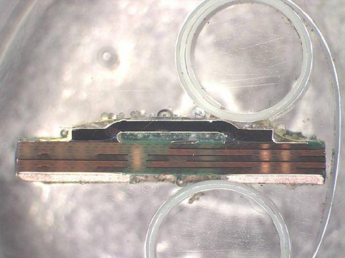
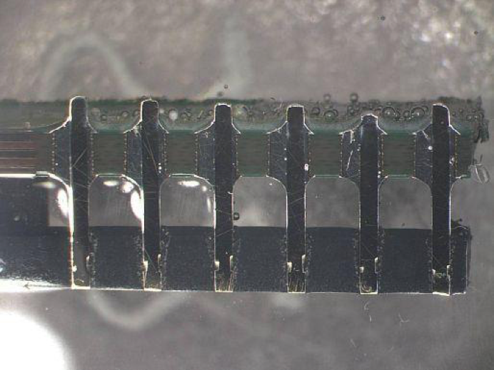
As inspection often will require further evaluation (destructive) per IPC-TM-650, the target areas of the board, component, pin through hole (PTH), via, terminal, solder joint, etc. will be isolated for analysis. The area will be cut and removed from the PCB and the cross-section analysis plane identified. The section will be mounted in an epoxy and carefully ground to the target plane. Often times this can be successive plane evaluation as well. Once the analysis plane has been reached, the mounted specimen will be further prepared for the specific feature of interest. The most common features of interest in these evaluations are crack and void evaluation in a solder joint and plating thickness and roughness measurements.
The features are photo-documented and measured at microscopic magnifications either specified or appropriate for the feature.
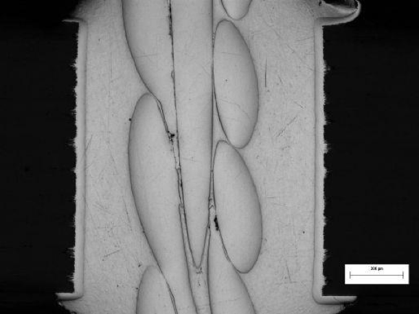
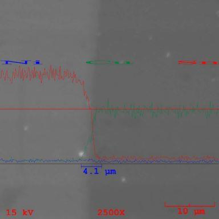
A particular feature of interest might be to determine the thickness of an intermetallic layer formation, or presence of microscopic dendrite or crystal whisker formation. At this point a prepared specimen can be analyzed by SEM (Scanning Electron Microscopy) and EDS (Energy Dispersive X-ray Spectroscopy) to obtain high magnification imaging and spatially resolved elemental composition to measure the feature. The SEM images, EDS spectra, X-ray dot maps and/or line profile analysis will be provided to document the feature annotated with measurement data when appropriate.
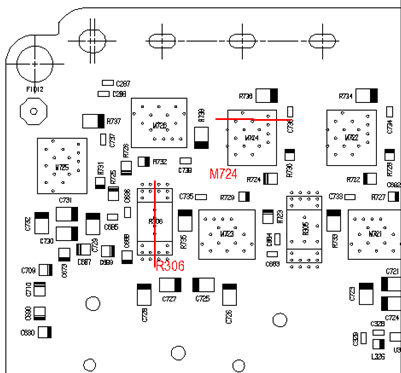
For RTI to adequately assess the needs of the client for PCBA, we will ask that photographs or drawings of the PCB be submitted with the request and the target plane(s) identified with a line through the area as seen below. The target feature or IPC (or other) inspection criteria should also be specified.
Additional services offered relating to Printed Circuit Board Analysis include the following:
- FTIR-microscopic (Fourier Transform Infrared Spectroscopy) analysis for identification of organic micro-constituents
- Component and board cleanliness testing for particulate or ionic residues
- PCB composition analysis for resin, filler, additive type and concentrations
- RoHS compliance testing