SEM/EDS Analysis
Scanning electron microscopy (SEM) and energy dispersive X-ray spectroscopy (EDS) allow for targeted analysis of sample surfaces. These techniques are widely used for material surface analysis, investigation of product failures, reverse engineering, contaminant identification, solder joint analysis and more. RTI Laboratories has professionals experienced with SEM and EDS analysis for all of your analytical needs. Contact us to request a quote.
What is Scanning Electron Microscopy (SEM)?
Scanning electron microscopy (SEM) and energy dispersive x-ray spectroscopy (EDS) comprise what has long been the “advanced” surface analysis tool for the materials scientist. Since commercial development in the 1950s, several significant technological advances have been made, however, the underlying physics of these methods remain the same.

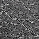
SEM is the imaging portion of the technique. While a “regular” optical microscope utilizes light for imaging, a scanning electron microscope uses electrons—essentially translating electron interactions into an optical signal. While optical microscopy has its advantages for certain applications, there can be resolution limitations, ultimately defined by light wavelength and low focal depth. However, with SEM, magnification and resolution are ultimately defined by the electron optics and sample interaction, allowing for a larger depth of focus.
How Does Scanning Electron Microscopy (SEM) Work?
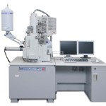
The physical process behind SEM is relatively simple and resembles that of a glorified cathode ray tube. The electrons are generated at the cathode by passing current through a metallic filament. The generated electrons are then accelerated towards the anode using high voltage. At the anode, the electron beam is collimated through a series of fine apertures and generated electromagnetic fields that surround the column. The electron beam ultimately exits the column directed towards the sample surface. When the contiguous beam hits the sample, several physical phenomena occur, however, we primarily focus on two of those physical interactions for imaging: generation of secondary electrons and backscattered electrons.
- Secondary electrons are generated from the sample itself, yielded by the energy of the incident beam electrons. The secondary electrons are “gathered” by an off axis detector that utilizes the secondary electron to fluoresce a scintillating material on the detector face, much like a cathode ray tube would use phosphorus to fluoresce on a TV screen. The fluoresced material on the detector face is then translated to an electronic signal using a photomultiplier tube. The positioning of that electron signal is determined by “scanning” the sample with the electron beam and the detector signal is coupled to that of the incident beam position.
- Backscattered electrons are not generated in the sample. They are the incident electrons that bounce around in the sample and then return out of the sample.
Backscattered electrons have much lower energies than secondary electrons and we primarily utilize them to help identify areas of differing mean atomic number, due to their ability to show differences in absorption between elements.
Scanning Electron Microscopy (SEM) Capabilities and Technological Advancements

Because SEM uses excited electrons for imaging, the electron microscope must act in a high vacuum environment such that the electrons are not absorbed by the atmospheric molecules as they move to the sample and detector. For this reason, we must consider the behavior of the sample under high vacuum conditions, thus liquids and biologics are normally precluded from analysis. Additionally, the sample must be able to complete an electrical circuit, meaning it must be conductive or made to be conductive by sputter coating (application of a “thin film” of conductive material).
Many of the technological advances throughout the years have sought to allow for SEM analysis to be performed in low vacuum conditions, with less surface conductance. The computerization and digitization of image acquisition has also contributed substantially to the expansion of SEM analysis capabilities.
What is Energy Dispersive X-ray Spectroscopy (EDS)?
A number of physical phenomena, in addition to the electron interactions used for imaging, take place at the sample surface. It is possible to take advantage of these interactions to obtain chemical information. As secondary electrons are generated for imaging, the interacted atom becomes ionized and must capture an outer shell electron to return to the ground state. Per the law of conservation of energy, a photon is then emitted which is characteristic of the shell transition that occurred and is “quantized” as defined by the rules of quantum mechanics. We measure the energy of that emitted photon and essentially “look it up” for the energy transitions that occur for each element. The EDS detector is the tool we utilize for measuring the energy of the emitted photons in the X-ray electromagnetic spectrum.

The detector is a solid state chip or crystal that is cooled to superconducting temperature for high quantum efficiency and is off axis from the incident beam.
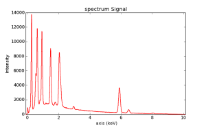
The detected X-rays are segregated into energy channels based on their interaction with the detector, and form a spectrum of detected energies. With the spectrum, we can identify the peak energies and determine what electron transition occurred and thus what element it corresponds to. We can also couple this data to the SEM imaging technique to form X-ray “maps” of data to overlay or present areas of high individual elemental concentrations.
Technological Advancements in Energy Dispersive X-ray Spectroscopy (EDS)
Technological advances in EDS analysis have come in the form of making detectors that don’t need to be cooled with liquid nitrogen to superconduct. In addition, higher efficiency chips have been fabricated along with processing electronics that have resulted in throughput improvements of over 1000 times conventional detectors. An improved understanding of X-ray intensity data has also given rise to fairly accurate quantitative algorithms. Lastly, improvements in software and computing capabilities have helped to make EDS analysis more efficient.
When are Scanning Electron Microscopy (SEM) and Energy Dispersive X-ray Spectroscopy (EDS)Used?
So with all that being said, what do we do with these high dollar instruments? Well, just about anything! SEM and EDS analysis are used virtually anywhere we need to obtain a high resolution, high depth of field image as well as an elemental composition for a bulk material, or a particular area of that material. In the lab we have developed procedures around a wide variety of particular analysis requirements, such as:
- Fractography and failure analysis of parts, metals, and plastics.
- Surface features analysis for micro-constituents or micro-inclusion content.
- Identification and quantitation of surface crystal morphology for metallic conversion coatings.
- Particle size and composition distribution analysis.
- Paint contaminant identification.
- Identification of organic to metal bonding failure modes.
- Characterization of intermetallic distribution in solder interfaces (printed circuit boards).
- Characterization of intermetallic distribution in metallic coating interfaces.
- Unknown materials identification.
- Alloy phase identification.
- Coating thickness and uniformity measurements.
- Forensic investigations to determine materials source.
What Industries and Companies Need Scanning Electron Microscopy (SEM) and Energy Dispersive X-ray Spectroscopy (EDS) Analysis?

As SEM and EDS analysis are primarily investigative approaches, industry standard methodologies tend to be non-existent or irrelevant. The techniques are tailored to a particular application or scientific dilemma based upon the objective of the scientist.
It seems no industry is immune to utilization of SEM and EDS in routine or investigative analysis.
The techniques are used by clients in fundamental research, automotive OEM and suppliers, metals processing, plastics manufacturing and fabrication, paints and coatings manufacturing and application, pharmaceutical, medical devices manufacturing and cleaning, filtration specialists and design, electronics components and printed circuit board manufacturers, to name a few.
New procedures are developed constantly, so it is never too crazy to ask whether SEM and EDS analysis are appropriate. SEM and EDS analysis are often the techniques we first turn to when someone asks, “What is this?”

